Intel has introduced Sunny Cove as a new processor architecture. The architecture is used for the first time in Ice Lake and relies on a multi-chip design.
Sunny Cove is Intel’s new CPU architecture
Intel today unveiled the new Sunny Cove processor architecture at Architecture Day. It inherits the Skylake architecture, which was used for the first time in the Skylake processor series with the same name. However, there is no name change with Sunny Cove. The architecture is to be used for the first time in the Ice Lake series. The processors are to be launched on the market at the end of 2019. With Sunny Cove, there are some innovations in the internal structure that Intel is supposed to arm against AMD’s Zen 2 architecture, which will be used for the first time in Epyc 2 alias Rome and Ryzen 3000.
More parallelization and more IPC
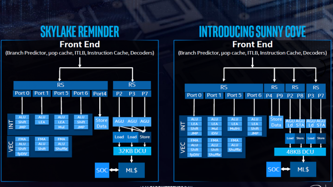
As in previous generations, the IPC in particular should improve significantly. Intel wants to extend its lead over AMD once again. This should work by a combination of fast and more cache memory and a better command management. The L1 cache is increased from 32 to 48 kilobytes by 50 percent. The L2 cache will also be larger, but Intel does not yet give any exact details. With Sunny Cove, two loads and stores should also be possible per clock cycle, while the Lake architecture only managed one load and one store each. This allows significantly more data and commands per clock to be passed on to the execution units, which increases the IPC.
With Sunny Cove, Intel is also for the first time focusing on more parallelization. Instead of four, there are now five allocators and 10 instead of 8 ports for the arithmetic units. There is also one more address generator, which is why a total of four AGUs (Address Generation Units) are now installed. In addition, there are now two store units instead of one for writing back after executing commands. The Instructions Per Cycle are especially important for applications that use only a few threads and accelerate these applications enormously. Combined with a clock rate of 5 GHz, initial estimates suggest that between 20 and 30 percent more IPC will be possible. The strong increase can also be seen in a demonstration with 7-Zip, in which an Ice Lake prototype calculated 75 percent faster than its predecessor. However, the demonstration had been shown without further information such as the clock speed and is therefore still difficult to estimate.
Foveros: Intel also relies on a multi-chip design
While AMD already relied on a multi-chip design with the first Zen generation, Intel still held back. In the meantime the Epyc processors were discredited as “four desktop processors glued together”. However, Intel’s Architecture Day also shows that this approach has a future. With Sunny Cove, the MCM approach is also to be used on a large scale at Intel. The new design for processors is called Intel Foveros. It could be used in all processor types, from tablets to servers.
While AMD positions and connects the chips next to each other, Intel stacks different chips on top of each other with Foveros. The EMIB technology is used as the connection. The interposer, which connects all the elements, is located at the bottom of an ordinary package. The various chips then sit on top. On the one hand, there should be x86 chips connected to the interposer via silicon. On the other hand, other chips can also be placed on top of the interposer. For tablets, for example, it is possible to connect an LTE modem. The RAM can also be packed directly onto the interposer. The power supply for all chips works directly via the interposer.
In this approach, the interposer itself is a 22nm chip. The x86 chips are already produced with 10nm. As with AMD’s Epyc 2, the interposer could also take over I/O and memory management. However, Intel has not yet confirmed this. Also FPGA chiplets for the server area find place on the interposer. Other possible applications are discrete graphics chiplets. Intel already has experience with this through Kaby Lake-G, on whose package an AMD-GPU was soldered. Further details are not expected until 2019.
New iGPU creates 1 TFLOP for the first time
With the new Sunny Cove architecture also a new iGPU generation comes with the simple name Gen11. The iGPUs have never been really powerful, the Gen11 is supposed to change that at least in part. The new iGPU should reach a TFLOP of computing power from now on. This is of course no comparison to real gaming graphics cards, but integrated graphics units were never suitable for really complex gaming. With Raven Ridge and a good 1.7 TFLOPs, AMD has presented a clear example, but for real gaming fun you will still need a dedicated graphics card.
Nevertheless, the increase in performance is not to be despised. Compared to the current Coffee Lake Refresh generation, which still includes the Gen9.5-iGPU, the performance increases by a good 100 percent. Intel uses 64 shader blocks for this purpose, while only 24 were used in the Gen9. With Coarse Pixel Shading (CPS), performance also increases. In shooters, for example, the GPU only accurately calculates the central image part, while the remaining image parts are calculated with significantly reduced quality. Especially with fast games like shooters this can be an advantage, as the player only concentrates on the central part anyway. With the new iGPU, Intel once again confirms the support of Adaptive Sync, which is called FreeSync in AMD. This makes tearing a thing of the past.

Be the first to comment